Hysteresis
Thyristors are a class of semiconductor components exhibiting hysteresis, that property whereby
a system fails to return to its original state after some cause of state change has been removed.
A very simple example of hysteresis is the mechanical action of a toggle switch: when the
lever is pushed, it flips to one of two extreme states (positions) and will remain there even
after the source of motion is removed (after you remove your hand from the switch lever). To
illustrate the absence of hysteresis, consider the action of a ”momentary” pushbutton switch,
which returns to its original state after the button is no longer pressed: when the stimulus is
removed (your hand), the system (switch) immediately and fully returns to its prior state with
no ”latching” behavior.
Bipolar, junction field-effect, and insulated gate field-effect transistors are all non-hysteric
devices. That is, these do not inherently ”latch” into a state after being stimulated by a voltage
or current signal. For any given input signal at any given time, a transistor will exhibit a predictable output response as defined by its characteristic curve. Thyristors, on the other
hand, are semiconductor devices that tend to stay ”on” once turned on, and tend to stay ”off ”
once turned off. A momentary event is able to flip these devices into either their on or off
states where these will remain that way on their own, even after the cause of the state change
is taken away. As such, these are useful only as on/off switching devices – much like a toggle
switch – and cannot be used as analog signal amplifiers.
Thyristors are constructed using the same technology as bipolar junction transistors, and
in fact may be analyzed as circuits comprised of transistor pairs. How then, can a hysteric device
(a thyristor) be made from non-hysteric devices (transistors)? The answer to this question
is positive feedback, also known as regenerative feedback. As you should recall, feedback is the
condition where a percentage of the output signal is ”fed back” to the input of an amplifying
device. Negative, or degenerative, feedback results in a diminishing of voltage gain with increases
in stability, linearity, and bandwidth. Positive feedback, on the other hand, results in
a kind of instability where the amplifier’s output tends to ”saturate.” In the case of thyristors,
this saturating tendency equates to the device ”wanting” to stay on once turned on, and off
once turned off.
In this chapter we will explore several different kinds of thyristors, most of which stem from
a single, basic two-transistor core circuit. Before we do that, though, it would be beneficial to
study the technological predecessor to thyristors: gas discharge tubes.
Gas discharge tubes:
If you’ve ever witnessed a lightning storm, you’ve seen electrical hysteresis in action (and
probably didn’t realize what you were seeing). The action of strong wind and rain accumulates
tremendous static electric charges between cloud and earth, and between clouds as well.
Electric charge imbalances manifest themselves as high voltages, and when the electrical resistance
of air can no longer hold these high voltages at bay, huge surges of current travel
between opposing poles of electrical charge which we call ”lightning.”
The buildup of high voltages by wind and rain is a fairly continuous process, the rate of
charge accumulation increasing under the proper atmospheric conditions. However, lightning
bolts are anything but continuous: they exist as relatively brief surges rather than continuous
discharges. Why is this? Why don’t we see soft, glowing lightning arcs instead of violently brief
lightning bolts? The answer lies in the nonlinear (and hysteric) resistance of air.
Under ordinary conditions, air has an extremely high amount of resistance. It is so high, in
fact, that we typically treat its resistance as infinite and electrical conduction through the air
as negligible. The presence of water and dust in air lowers its resistance some, but it is still an
insulator for most practical purposes. When enough high voltage is applied across a distance
of air, though, its electrical properties change: electrons become ”stripped” from their normal
positions around their respective atoms and are liberated to constitute a current. In this state,
air is considered to be ionized and is called a plasma rather than a gas. This usage of the word
”plasma” is not to be confused with the medical term (meaning the fluid portion of blood), but
is a fourth state of matter, the other three being solid, liquid, and vapor (gas). Plasma is a
relatively good conductor of electricity, its specific resistance being much lower than that of the
same substance in its gaseous state.
As an electric current moves through the plasma, there is energy dissipated in the plasma in the formof heat, just as current through a solid resistor dissipates energy in the formof heat.
In the case of lightning, the temperatures involved are extremely high. High temperatures are
also sufficient to convert gaseous air into a plasma or maintain plasma in that state without
the presence of high voltage. As the voltage between cloud and earth, or between cloud and
cloud, decreases as the charge imbalance is neutralized by the current of the lightning bolt, the
heat dissipated by the bolt maintains the air path in a plasma state, keeping its resistance low.
The lightning bolt remains a plasma until the voltage decreases to too low a level to sustain
enough current to dissipate enough heat. Finally, the air returns to a gaseous state and stops
conducting current, thus allowing voltage to build up once more.
Note how throughout this cycle, the air exhibits hysteresis. When not conducting electricity,
it tends to remain an insulator until voltage builds up past a critical threshold point. Then,
once it changes state and becomes a plasma, it tends to remain a conductor until voltage falls
below a lower critical threshold point. Once ”turned on” it tends to stay ”on,” and once ”turned
off ” it tends to stay ”off.” This hysteresis, combined with a steady buildup of voltage due to the
electrostatic effects of wind and rain, explains the action of lightning as brief bursts.
In electronic terms, what we have here in the action of lightning is a simple relaxation oscillator.
Oscillators are electronic circuits that produce an oscillating (AC) voltage from a steady
supply of DC power. A relaxation oscillator is one that works on the principle of a charging
capacitor that is suddenly discharged every time its voltage reaches a critical threshold value.
One of the simplest relaxation oscillators in existence is comprised of three components (not
counting the DC power supply): a resistor, capacitor, and neon lamp in Figure

Figure: Simple relaxation oscillator
Neon lamps are nothing more than two metal electrodes inside a sealed glass bulb, separated
by the neon gas inside. At room temperatures and with no applied voltage, the lamp
has nearly infinite resistance. However, once a certain threshold voltage is exceeded (this voltage
depends on the gas pressure and geometry of the lamp), the neon gas will become ionized
(turned into a plasma) and its resistance dramatically reduced. In effect, the neon lamp exhibits
the same characteristics as air in a lightning storm, complete with the emission of light
as a result of the discharge, albeit on a much smaller scale.
The capacitor in the relaxation oscillator circuit shown above charges at an inverse exponential
rate determined by the size of the resistor. When its voltage reaches the threshold
voltage of the lamp, the lamp suddenly ”turns on” and quickly discharges the capacitor to a
low voltage value. Once discharged, the lamp ”turns off ” and allows the capacitor to build up a charge once more. The result is a series of brief flashes of light from the lamp, the rate of which
is dictated by battery voltage, resistor resistance, capacitor capacitance, and lamp threshold
voltage.
While gas-discharge lamps are more commonly used as sources of illumination, their hysteric
properties were leveraged in slightly more sophisticated variants known as thyratron
tubes. Essentially a gas-filled triode tube (a triode being a three-element vacuum electron tube
performing much a similar function to the N-channel, D-type IGFET), the thyratron tube could
be turned on with a small control voltage applied between grid and cathode, and turned off by
reducing the plate-to-cathode voltage.

Figure: Simple thyratron control circuit
In essence, thyratron tubes were controlled versions of neon lamps built specifically for
switching current to a load. The dot inside the circle of the schematic symbol indicates a gas
fill, as opposed to the hard vacuum normally seen in other electron tube designs. In the circuit
shown above in Figure . the thyratron tube allows current through the load in one direction
(note the polarity across the load resistor) when triggered by the small DC control voltage
connected between grid and cathode. Note that the load’s power source is AC, which provides a
clue about how the thyratron turns off after its been triggered on: since AC voltage periodically
passes through a condition of 0 volts between half-cycles, the current through an AC-powered
load must also periodically halt. This brief pause of current between half-cycles gives the
tube’s gas time to cool, letting it return to its normal ”off ” state. Conduction may resume only
if enough voltage is applied by the AC power source (some other time in the wave’s cycle) and
if the DC control voltage allows it.
An oscilloscope display of load voltage in such a circuit would look something like Figure.
As the AC supply voltage climbs from zero volts to its first peak, the load voltage remains
at zero (no load current) until the threshold voltage is reached. At that point, the tube switches
”on” and begins to conduct, the load voltage now following the AC voltage through the rest of
the half cycle. Load voltage exists (and thus load current) even when the AC voltage waveform
has dropped below the threshold value of the tube. This is hysteresis at work: the tube stays
in its conductive mode past the point where it first turned on, continuing to conduct until
there the supply voltage drops off to almost zero volts. Because thyratron tubes are one-way
(diode) devices, no voltage develops across the load through the negative half-cycle of AC.

Figure: Thyratron waveforms
In practical thyratron circuits, multiple tubes arranged in some form of full-wave rectifier circuit
to facilitate full-wave DC power to the load.
The thyratron tube has been applied to a relaxation oscillator circuit. [1] The frequency
is controlled by a small DC voltage between grid and cathode. (See Figure) This voltagecontrolled
oscillator is known as a VCO. Relaxation oscillators produce a very non-sinusoidal
output, and they exist mostly as demonstration circuits (as is the case here) or in applications
where the harmonic rich waveform is desirable.

Figure: Voltage controlled thyratron relaxation oscillator
have obsoleted thyratron tube technology for all but a few very special applications. It
is no coincidence that the word thyristor bears so much similarity to the word thyratron, for
this class of semiconductor components does much the same thing: use hysteretically switch
current on and off. It is these modern devices that we now turn our attention to.
• REVIEW:
• Electrical hysteresis, the tendency for a component to remain ”on” (conducting) after it
begins to conduct and to remain ”off ” (nonconducting) after it ceases to conduct, helps to
explain why lightning bolts exist as momentary surges of current rather than continuous
discharges through the air.
• Simple gas-discharge tubes such as neon lamps exhibit electrical hysteresis.
• More advanced gas-discharge tubes have been made with control elements so that theirbegins to conduct and to remain ”off ” (nonconducting) after it ceases to conduct, helps to
explain why lightning bolts exist as momentary surges of current rather than continuous
discharges through the air.
• Simple gas-discharge tubes such as neon lamps exhibit electrical hysteresis.
”turn-on” voltage could be adjusted by an external signal. The most common of these
tubes was called the thyratron.
• Simple oscillator circuits called relaxation oscillators may be created with nothing more
than a resistor-capacitor charging network and a hysteretic device connected across the
capacitor.
The Shockley Diode:
Our exploration of thyristors begins with a device called the four-layer diode, also known as
a PNPN diode, or a Shockley diode after its inventor, William Shockley. This is not to be
confused with a Schottky diode, that two-layer metal-semiconductor device known for its high
switching speed. A crude illustration of the Shockley diode, often seen in textbooks, is a fourlayer
sandwich of P-N-P-N semiconductor material, Figure

Figure: Shockley or 4-layer diode
Unfortunately, this simple illustration does nothing to enlighten the viewer on how it works
or why. Consider an alternative rendering of the device’s construction in Figure
or why. Consider an alternative rendering of the device’s construction in Figure
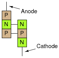
Figure: Transistor equivalent of Shockley diode
Let’s connect one of these devices to a source of variable voltage and see what happens:

Figure: Powered Shockley diode equivalent circuit.
With no voltage applied, of course there will be no current. As voltage is initially increased,
there will still be no current because neither transistor is able to turn on: both will be in cutoff
mode. To understand why this is, consider what it takes to turn a bipolar junction transistor
on: current through the base-emitter junction. As you can see in the diagram, base current
through the lower transistor is controlled by the upper transistor, and the base current through
the upper transistor is controlled by the lower transistor. In other words, neither transistor
can turn on until the other transistor turns on. What we have here, in vernacular terms, is
known as a Catch-22.
So how can a Shockley diode ever conduct current, if its constituent transistors stubbornly
maintain themselves in a state of cutoff? The answer lies in the behavior of real transistors
as opposed to ideal transistors. An ideal bipolar transistor will never conduct collector current
if no base current flows, no matter how much or little voltage we apply between collector and emitter. Real transistors, on the other hand, have definite limits to how much collector-emitter
voltage each can withstand before one breaks down and conduct. If two real transistors are
connected in this fashion to form a Shockley diode, each one will conduct if sufficient voltage is
applied by the battery between anode and cathode to cause one of them to break down. Once
one transistor breaks down and begins to conduct, it will allow base current through the other
transistor, causing it to turn on in a normal fashion, which then allows base current through
the first transistor. The end result is that both transistors will be saturated, now keeping each
other turned on instead of off.
So, we can force a Shockley diode to turn on by applying sufficient voltage between anode
and cathode. As we have seen, this will inevitably cause one of the transistors to turn on, which
then turns the other transistor on, ultimately ”latching” both transistors on where each will
tend to remain. But how do we now get the two transistors to turn off again? Even if the applied
voltage is reduced to a point well below what it took to get the Shockley diode conducting, it
will remain conducting because both transistors now have base current to maintain regular,
controlled conduction. The answer to this is to reduce the applied voltage to a much lower point
where too little current flows to maintain transistor bias, at which point one of the transistors
will cutoff, which then halts base current through the other transistor, sealing both transistors
in the ”off ” state as each one was before any voltage was applied at all.
If we graph this sequence of events and plot the results on an I/V graph, the hysteresis
is evident. First, we will observe the circuit as the DC voltage source (battery) is set to zero
voltage:

Figure: Zero applied voltage; zero current
Next, we will steadily increase the DC voltage. Current through the circuit is at or nearly
at zero, as the breakdown limit has not been reached for either transistor:
at zero, as the breakdown limit has not been reached for either transistor:
When the voltage breakdown limit of one transistor is reached, it will begin to conduct
collector current even though no base current has gone through it yet. Normally, this sort
of treatment would destroy a bipolar junction transistor, but the PNP junctions comprising a
Shockley diode are engineered to take this kind of abuse, similar to the way a Zener diode is
built to handle reverse breakdown without sustaining damage. For the sake of illustration I’ll
assume the lower transistor breaks down first, sending current through the base of the upper
transistor.
As the upper transistor receives base current, it turns on as expected. This action allows
the lower transistor to conduct normally, the two transistors ”sealing” themselves in the ”on”

Figure: Some applied voltage; still no current

Figure: More voltage applied; lower transistor breaks down
Full current is quickly seen in the circuit:

Figure: Transistors are now fully conducting.
The positive feedback mentioned earlier in this chapter is clearly evident here. When one
transistor breaks down, it allows current through the device structure. This current may be
viewed as the ”output” signal of the device. Once an output current is established, it works
to hold both transistors in saturation, thus ensuring the continuation of a substantial output
current. In other words, an output current ”feeds back” positively to the input (transistor base
current) to keep both transistors in the ”on” state, thus reinforcing (or regenerating) itself.
With both transistors maintained in a state of saturation with the presence of ample base
current, each will continue to conduct even if the applied voltage is greatly reduced from the
breakdown level. The effect of positive feedback is to keep both transistors in a state of saturation
despite the loss of input stimulus (the original, high voltage needed to break down one
transistor and cause a base current through the other transistor):

Figure: Current maintained even when voltage is reduced
If the DC voltage source is turned down too far, though, the circuit will eventually reach a
point where there isn’t enough current to sustain both transistors in saturation. As one transistor
passes less and less collector current, it reduces the base current for the other transistor,
thus reducing base current for the first transistor. The vicious cycle continues rapidly until
both transistors fall into cutoff: Here, positive feedback is again at work: the fact that the cause/effect cycle between both transistors is ”vicious” (a decrease in current through one works to decrease current through
the other, further decreasing current through the first transistor) indicates a positive relationship
between output (controlled current) and input (controlling current through the transistors’
bases).
The resulting curve on the graph is classically hysteretic: as the input signal (voltage) is
increased and decreased, the output (current) does not follow the same path going down as it
did going up: Put in simple terms, the Shockley diode tends to stay on once its turned on, and stay off
once its turned off. No ”in-between” or ”active” mode in its operation: it is a purely on or off
device, as are all thyristors.
A few special terms apply to Shockley diodes and all other thyristor devices built upon the
Shockley diode foundation. First is the term used to describe its ”on” state: latched. The word
”latch” is reminiscent of a door lock mechanism, which tends to keep the door closed once it has
been pushed shut. The term firing refers to the initiation of a latched state. To get a Shockley
diode to latch, the applied voltage must be increased until breakover is attained. Though this
action is best described as transistor breakdown, the term breakover is used instead because
the result is a pair of transistors in mutual saturation rather than destruction of the transistor.
A latched Shockley diode is re-set back into its nonconducting state by reducing current
through it until low-current dropout occurs.
Note that Shockley diodes may be fired in a way other than breakover: excessive voltage rise, or dv/dt. If the applied voltage across the diode increases at a high rate of change, it
may trigger. This is able to cause latching (turning on) of the diode due to inherent junction
capacitances within the transistors. Capacitors, as you may recall, oppose changes in voltage
by drawing or supplying current. If the applied voltage across a Shockley diode rises at too
fast a rate, those tiny capacitances will draw enough current during that time to activate the
transistor pair, turning them both on. Usually, this form of latching is undesirable, and can be
minimized by filtering high-frequency (fast voltage rises) from the diode with series inductors
and parallel resistor-capacitor networks called snubbers:

Figure: Both the series inductor and parallel resistor-capacitor “snubber” circuit help
minimize the Shockley diode’s exposure to excessively rising voltage.
minimize the Shockley diode’s exposure to excessively rising voltage.
The voltage rise limit of a Shockley diode is referred to as the critical rate of voltage rise.
Manufacturers usually provide this specification for the devices they sell.
Manufacturers usually provide this specification for the devices they sell.
• REVIEW:
• Shockley diodes are four-layer PNPN semiconductor devices. These behave as a pair of
interconnected PNP and NPN transistors.
• Like all thyristors, Shockley diodes tend to stay on once turned on (latched), and stay off
once turned off.
• To latch a Shockley diode exceed the anode-to-cathode breakover voltage, or exceed the
anode-to-cathode critical rate of voltage rise.
• To cause a Shockley diode to stop conducting, reduce the current going through it to a
level below its low-current dropout threshold
The DIAC
Like all diodes, Shockley diodes are unidirectional devices; that is, these only conduct current
in one direction. If bidirectional (AC) operation is desired, two Shockley diodes may be joined
in parallel facing different directions to form a new kind of thyristor, the DIAC:
in one direction. If bidirectional (AC) operation is desired, two Shockley diodes may be joined
in parallel facing different directions to form a new kind of thyristor, the DIAC:
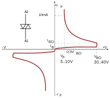
A DIAC operated with a DC voltage across it behaves exactly the same as a Shockley diode.
With AC, however, the behavior is different from what one might expect. Because alternating
current repeatedly reverses direction, DIACs will not stay latched longer than one-half cycle. If
a DIAC becomes latched, it will continue to conduct current only as long as voltage is available
to push enough current in that direction. When the AC polarity reverses, as it must twice
per cycle, the DIAC will drop out due to insufficient current, necessitating another breakover
before it conducts again. The result is the current waveform in Figure
DIACs are almost never used alone, but in conjunction with other thyristor devices.

The Silicon-Controlled Rectifier (SCR):
Shockley diodes are curious devices, but rather limited in application. Their usefulness may
be expanded, however, by equipping them with another means of latching. In doing so, each
becomes true amplifying devices (if only in an on/off mode), and we refer to these as siliconcontrolled
rectifiers, or SCRs. The progression from Shockley diode to SCR is achieved with one small addition, actually nothing more than a third wire connection to the existing PNPN structure:
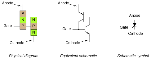
Figure: The Silicon-Controlled Rectifier (SCR)
If an SCR’s gate is left floating (disconnected), it behaves exactly as a Shockley diode. It
may be latched by breakover voltage or by exceeding the critical rate of voltage rise between
anode and cathode, just as with the Shockley diode. Dropout is accomplished by reducing
current until one or both internal transistors fall into cutoff mode, also like the Shockley diode.
However, because the gate terminal connects directly to the base of the lower transistor, it
may be used as an alternative means to latch the SCR. By applying a small voltage between
gate and cathode, the lower transistor will be forced on by the resulting base current, which
will cause the upper transistor to conduct, which then supplies the lower transistor’s base
with current so that it no longer needs to be activated by a gate voltage. The necessary gate
current to initiate latch-up, of course, will be much lower than the current through the SCR
from cathode to anode, so the SCR does achieve a measure of amplification.
This method of securing SCR conduction is called triggering, and it is by far the most common
way that SCRs are latched in actual practice. In fact, SCRs are usually chosen so that
their breakover voltage is far beyond the greatest voltage expected to be experienced from the
power source, so that it can be turned on only by an intentional voltage pulse applied to the
gate.
It should be mentioned that SCRs may sometimes be turned off by directly shorting their
gate and cathode terminals together, or by ”reverse-triggering” the gate with a negative voltage
(in reference to the cathode), so that the lower transistor is forced into cutoff. I say this is
”sometimes” possible because it involves shunting all of the upper transistor’s collector current
past the lower transistor’s base. This current may be substantial, making triggered shut-off
of an SCR difficult at best. A variation of the SCR, called a Gate-Turn-Off thyristor, or GTO,
makes this task easier. But even with a GTO, the gate current required to turn it off may be
as much as 20% of the anode (load) current! The schematic symbol for a GTO is shown in the
following illustration.
SCRs and GTOs share the same equivalent schematics (two transistors connected in a
positive-feedback fashion), the only differences being details of construction designed to grant
the NPN transistor a greater than the PNP. This allows a smaller gate current (forward or
reverse) to exert a greater degree of control over conduction from cathode to anode, with the
PNP transistor’s latched state being more dependent upon the NPN’s than vice versa. The Gate-Turn-Off thyristor is also known by the name of Gate-Controlled Switch, or GCS.
A rudimentary test of SCR function, or at least terminal identification, may be performed
with an ohmmeter. Because the internal connection between gate and cathode is a single PN
junction, a meter should indicate continuity between these terminals with the red test lead on
the gate and the black test lead on the cathode like this
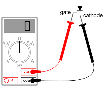
Figure: Rudimentary test of SCR
All other continuity measurements performed on an SCR will show ”open” (”OL” on some
digital multimeter displays). It must be understood that this test is very crude and does not
constitute a comprehensive assessment of the SCR. It is possible for an SCR to give good
ohmmeter indications and still be defective. Ultimately, the only way to test an SCR is to
subject it to a load current.
If you are using a multimeter with a ”diode check” function, the gate-to-cathode junction
voltage indication you get may or may not correspond to what’s expected of a silicon PN junction
(approximately 0.7 volts). In some cases, you will read a much lower junction voltage:
mere hundredths of a volt. This is due to an internal resistor connected between the gate and
cathode incorporated within some SCRs. This resistor is added to make the SCR less susceptible
to false triggering by spurious voltage spikes, from circuit ”noise” or from static electric
discharge. In other words, having a resistor connected across the gate-cathode junction requires
that a strong triggering signal (substantial current) be applied to latch the SCR. This feature is often found in larger SCRs, not on small SCRs. Bear in mind that an SCR with an
internal resistor connected between gate and cathode will indicate continuity in both directions
between those two terminals

Figure: Larger SCRs have gate to cathode resistor.
”Normal” SCRs, lacking this internal resistor, are sometimes referred to as sensitive gate
SCRs due to their ability to be triggered by the slightest positive gate signal.
The test circuit for an SCR is both practical as a diagnostic tool for checking suspected SCRs
and also an excellent aid to understanding basic SCR operation. A DC voltage source is used
for powering the circuit, and two pushbutton switches are used to latch and unlatch the SCR,
respectively.
Actuating the normally-open ”on” pushbutton switch connects the gate to the anode, allowing
current from the negative terminal of the battery, through the cathode-gate PN junction,
through the switch, through the load resistor, and back to the battery. This gate current should
force the SCR to latch on, allowing current to go directly from cathode to anode without further
triggering through the gate. When the ”on” pushbutton is released, the load should remain energized.
Pushing the normally-closed ”off ” pushbutton switch breaks the circuit, forcing current
through the SCR to halt, thus forcing it to turn off (low-current dropout).
If the SCR fails to latch, the problem may be with the load and not the SCR. A certain
minimum amount of load current is required to hold the SCR latched in the ”on” state. This
minimum current level is called the holding current. A load with too great a resistance value
may not draw enough current to keep an SCR latched when gate current ceases, thus giving
the false impression of a bad (unlatchable) SCR in the test circuit. Holding current values for
different SCRs should be available from the manufacturers. Typical holding current values
range from 1 milliamp to 50 milliamps or more for larger units.
For the test to be fully comprehensive, more than the triggering action needs to be tested.
The forward breakover voltage limit of the SCR could be tested by increasing the DC voltage
supply (with no pushbuttons actuated) until the SCR latches all on its own. Beware that
a breakover test may require very high voltage: many power SCRs have breakover voltage
ratings of 600 volts or more! Also, if a pulse voltage generator is available, the critical rate of
voltage rise for the SCR could be tested in the same way: subject it to pulsing supply voltages
of different V/time rates with no pushbutton switches actuated and see when it latches.
In this simple form, the SCR test circuit could suffice as a start/stop control circuit for a DC
motor, lamp, or other practical load.

Figure: DC motor start/stop control circuit
Another practical use for the SCR in a DC circuit is as a crowbar device for overvoltage
protection. A ”crowbar” circuit consists of an SCR placed in parallel with the output of a
DC power supply, for placing a direct short-circuit on the output of that supply to prevent
excessive voltage from reaching the load. Damage to the SCR and power supply is prevented
by the judicious placement of a fuse or substantial series resistance ahead of the SCR to limit
short-circuit current.Some device or circuit sensing the output voltage will be connected to the gate of the SCR,so that when an overvoltage condition occurs, voltage will be applied between the gate and
cathode, triggering the SCR and forcing the fuse to blow. The effect will be approximately the
same as dropping a solid steel crowbar directly across the output terminals of the power supply,
hence the name of the circuit.
Most applications of the SCR are for AC power control, despite the fact that SCRs are inherently
DC (unidirectional) devices. If bidirectional circuit current is required, multiple SCRs
may be used, with one or more facing each direction to handle current through both half-cycles
of the AC wave. The primary reason SCRs are used at all for AC power control applications
is the unique response of a thyristor to an alternating current. As we saw, the thyratron tube
(the electron tube version of the SCR) and the DIAC.
• REVIEW:
• A Silicon-Controlled Rectifier, or SCR, is essentially a Shockley diode with an extra terminal
added. This extra terminal is called the gate, and it is used to trigger the device
into conduction (latch it) by the application of a small voltage.
• To trigger, or fire, an SCR, voltage must be applied between the gate and cathode, positive
to the gate and negative to the cathode. When testing an SCR, a momentary connection
between the gate and anode is sufficient in polarity, intensity, and duration to trigger it.
• SCRsmay be fired by intentional triggering of the gate terminal, excessive voltage (breakdown)
between anode and cathode, or excessive rate of voltage rise between anode and cathode. SCRs may be turned off by anode current falling below the holding current value
(low-current dropout), or by ”reverse-firing” the gate (applying a negative voltage to the
gate). Reverse-firing is only sometimes effective, and always involves high gate current.
• A variant of the SCR, called a Gate-Turn-Off thyristor (GTO), is specifically designed to
be turned off by means of reverse triggering. Even then, reverse triggering requires fairly
high current: typically 20% of the anode current.
• SCR terminals may be identified by a continuity meter: the only two terminals showing
any continuity between them at all should be the gate and cathode. Gate and cathode
terminals connect to a PN junction inside the SCR, so a continuity meter should obtain
a diode-like reading between these two terminals with the red (+) lead on the gate and
the black (-) lead on the cathode. Beware, though, that some large SCRs have an internal
resistor connected between gate and cathode, which will affect any continuity readings
taken by a meter.
• SCRs are true rectifiers: they only allow current through them in one direction. This
means they cannot be used alone for full-wave AC power control.
• If the diodes in a rectifier circuit are replaced by SCRs, you have the makings of a controlled
rectifier circuit, whereby DC power to a load may be time-proportioned by triggering
the SCRs at different points along the AC power waveform.
The TRIAC:
SCRs are unidirectional (one-way) current devices, making them useful for controlling DC
only. If two SCRs are joined in back-to-back parallel fashion just like two Shockley diodes were
joined together to form a DIAC, we have a new device known as the TRIAC
only. If two SCRs are joined in back-to-back parallel fashion just like two Shockley diodes were
joined together to form a DIAC, we have a new device known as the TRIAC

Figure: The TRIAC SCR equivalent and, TRIAC schematic symbol
Because individual SCRs are more flexible to use in advanced control systems, these are
more commonly seen in circuits like motor drives; TRIACs are usually seen in simple, lowpower
applications like household dimmer switches.
more commonly seen in circuits like motor drives; TRIACs are usually seen in simple, lowpower
applications like household dimmer switches.
TRIACs are notorious for not firing symmetrically. This means these usually won’t trigger
at the exact same gate voltage level for one polarity as for the other. Generally speaking, this
is undesirable, because unsymmetrical firing results in a current waveform with a greater variety
of harmonic frequencies. Waveforms that are symmetrical above and below their average
centerlines are comprised of only odd-numbered harmonics. Unsymmetrical waveforms, on
the other hand, contain even-numbered harmonics (which may or may not be accompanied by
odd-numbered harmonics as well).
In the interest of reducing total harmonic content in power systems, the fewer and less
diverse the harmonics, the better – one more reason individual SCRs are favored over TRIACs
for complex, high-power control circuits. One way to make the TRIAC’s current waveform
more symmetrical is to use a device external to the TRIAC to time the triggering pulse. A
DIAC placed in series with the gate does a fair job of this

Figure: DIAC improves symmetry of control
DIAC breakover voltages tend to be much more symmetrical (the same in one polarity
as the other) than TRIAC triggering voltage thresholds. Since the DIAC prevents any gate
current until the triggering voltage has reached a certain, repeatable level in either direction,
the firing point of the TRIAC from one half-cycle to the next tends to be more consistent, and
the waveform more symmetrical above and below its centerline.
Practically all the characteristics and ratings of SCRs apply equally to TRIACs, except
that TRIACs of course are bidirectional (can handle current in both directions). Not much
more needs to be said about this device except for an important caveat concerning its terminal
designations.
• REVIEW:
• A TRIAC acts much like two SCRs connected back-to-back for bidirectional (AC) operation.
• TRIAC controls are more often seen in simple, low-power circuits than complex, highpower
circuits. In large power control circuits, multiple SCRs tend to be favored.
• When used to control AC power to a load, TRIACs are often accompanied by DIACs connected
in series with their gate terminals. The DIAC helps the TRIAC fire more symmetrically
(more consistently from one polarity to another).
• Main terminals 1 and 2 on a TRIAC are not interchangeable.
• To successfully trigger a TRIAC, gate current must come from the main terminal 2 (MT2)
side of the circuit!
This is a very good notes for the students who want to read about the Thyristors and the design.
ReplyDeleteI'am very thankful to you for reading this note about Thyristors !
ReplyDelete